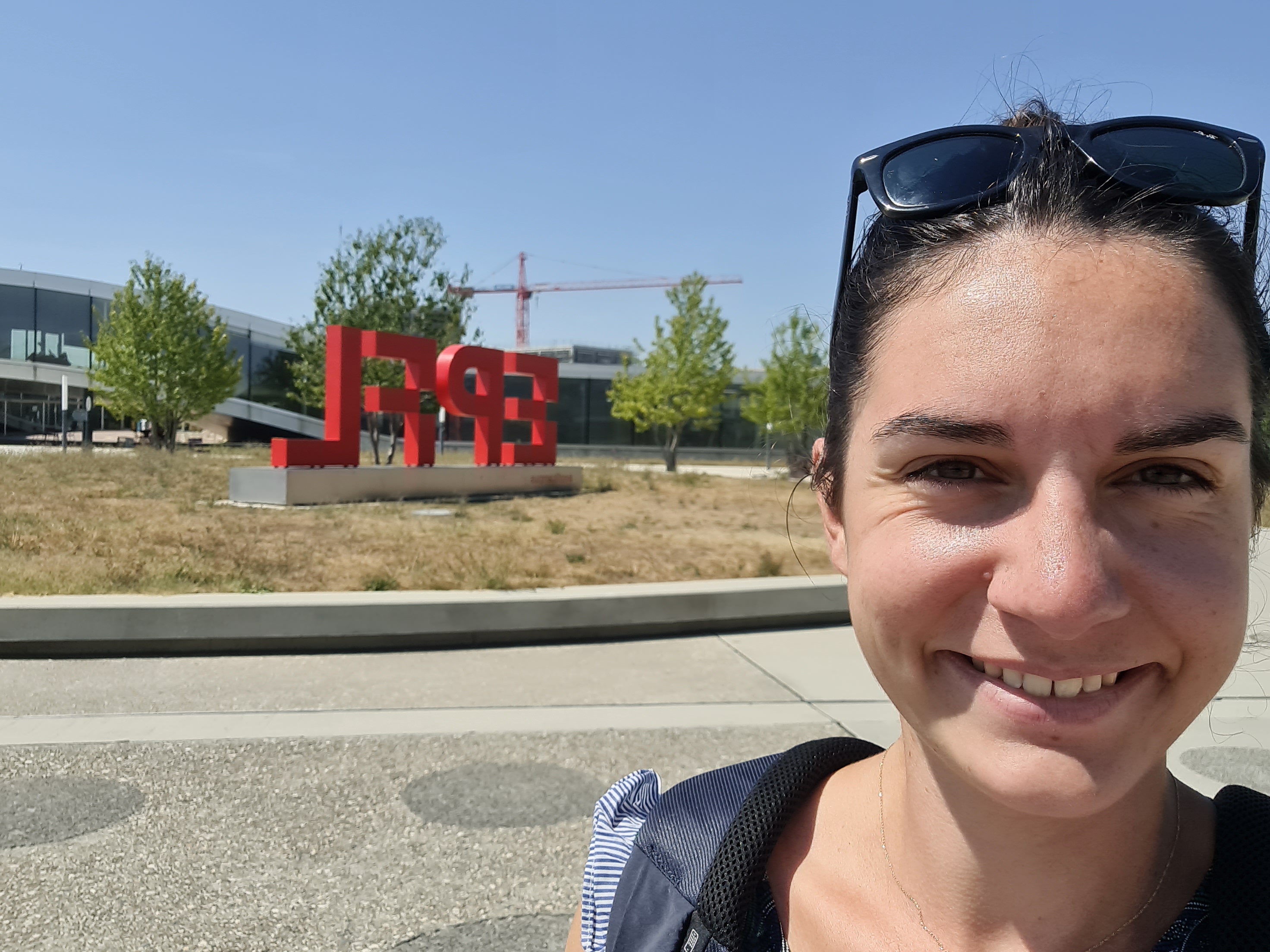
My internship took place in a laboratory belonging to the Ecole Polytechnique Fédérale de Lausanne (EPFL) called the Swiss Plasma Center (SPC). The main purpose of the SPC is to make ITER (International Thermonuclear Experimental Reactor) a success. Then, the following aim is to exploit the results obtained with ITER for use in DEMO (DEMOnstration power plant). ITER will prove that fusion can be made on Earth and DEMO will prove that fusion energy can be commercialized.
To maintain the fusion nuclear reaction, it is mandatory to well know what happens it the core of the reactor, in the plasma. The plasma is considered as the fourth state of matter. It is a gaseous assembly of electrons, ions and neutral particles. The charged particles of this plasma are confined thanks to a magnetic field. Thus, to understand in which state is the plasma and the magnetic field, it is necessary to collect data with sensors. I was therefore asked to study and design a probe for DEMO. The desire to reduce the size of the probe introduces further changes both the manufacturing process and the internal design of the probe.
To determine the state of the plasma, we can use magnetic coils that will gives us information about the magnetic field or its time derivated. The sensor I will use is basically a coil. This coil has different variable parameters. For instance, we can choose how many turns the coil will have, the geometry of the windings (circular, rectangular, ...). In my case, the windings were concentric, like a kind of spiral. The aim is for the plasma to be captured in the probe coils. Therefore, the largest possible surface area is required.
The purpose of the probe is to capture magnetic field in its windings. Increasing the number of turns increases the effective area. However, increasing the number of turns increases the impedance as this depends on N2.
The Low Temperature co-fired ceramics (LTCC) technique worked perfectly for the manufacture of the probes for ITER. However, having reduced the size of the tracks we can no longer use this technique. Indeed, the instruments that deposits the ink to create the metal track has a diameter that is too large now. Thus, we will use photolithography instead.
The photolithography is the process of transferring a particular pattern onto a substrate with light exposure, much like a negative image in standard photography. The different areas defined by the patterns will become the different areas of the electronic components. The laboratories we have at EPFL allows us to use different materials for the substrates, notably sapphire or silicon oxide. The ink used for the tracks will also be a variable parameter when creating the probes.
I was asked to model the probe to optimize its geometry. The impedance of a circuit is the total resistance of the cable to the electric current flowing through it. A calculation shows that reducing the wire size increases the effective area NAEFF, which is an effective value for the product of the number of turns, N, and the area, A. Indeed, we reach the same effective area as for ITER but with fewer turns. This is useful for us because inductance, which we want to minimize, varies with the number of turns squared.
These kinds of sensors will evolve in a complex environment subjected to high level of radiations. This is the reason why I try to reduce the size of the sensor as much as possible. In the near future, the probe will be made in real with different parameters. Some EPFL students are currently working in clean rooms to create the probe. Different types of wafers, different wire diameters, different track width will be tested.

